Synopsys Tutorial: Power Estimation
From CVL Wiki
| Line 3: | Line 3: | ||
By Syed Haider | By Syed Haider | ||
| + | == Note == | ||
| + | It has come to my attention that copying text from a wiki to text files sometimes leads | ||
| + | to the insertion of hidden characters. So if the tools experience trouble with the scripts | ||
| + | or hdl code copied from this wiki, just retype the files shown and the tools should have no trouble. | ||
== Setting Up Standard Cell Library and Project Directory == | == Setting Up Standard Cell Library and Project Directory == | ||
Revision as of 16:48, 14 February 2008
Power Estimation with OSU Standard Cell Library and Synopsys tools (PrimeTime-Px)
By Syed Haider
Contents |
Note
It has come to my attention that copying text from a wiki to text files sometimes leads to the insertion of hidden characters. So if the tools experience trouble with the scripts or hdl code copied from this wiki, just retype the files shown and the tools should have no trouble.
Setting Up Standard Cell Library and Project Directory
1. Download Oklahoma State University Library from http://vcag.ecen.okstate.edu/projects/scells/
Specifically, from: http://vcag.ecen.okstate.edu/projects/scells/download/iit_stdcells_v2.3beta/
Download the iitcells_lib_2.3.tar.gz package.
2. untar the library somewhere nice like your home directory where you will really never touch it (i.e. /home/syedh/). The Directory will be called iit_stdcells.
3. Create a project directory somewhere else. (example: mkdir /home/syedh/Project1) In Project1 create another directory called WORK.
4. Back in Project1 directory create an empty file called: .synopsys_dc.setup
This file will specify to Synopsys and design_vision software what libraries you are using. A sample version of the file is listed below. The path after “/home/syedh/” should remain unchanged if this tutorial is being followed correctly!!!
# .synopsys_dc.setup file
# Define the target tehcnology library, symbol library,
# and link libraries
set target_library /home/syedh/iit_stdcells/lib/tsmc018/lib/iit018_stdcells.db
#do not have a symbol library
#set symbol_library

#set link library (set as same as target library)

set link_library “/home/syedh/iit_stdcells/lib/tsmc018/lib/iit018_stdcells.db *”

set designer "Your Name"
5. Copy /home/syedh/iit_stdcells/lib/tsmc018/lib/iit018_stdcells.v into Project1 Directory.
Sample Design Example
6. Now it is design time. Create verilog description of something amazing. Here is a design of a full adder and some registers that spans multiple design files (full_adder.v, top.v):
//full_adder.v
//This is a module for a 1 bit Full Adder
module full_adder(a,b, c_in, s, c_out);

input a, b, c_in;
output wire s, c_out;

assign s = a ^ b ^ c_in;
assign c_out = ((a & b)) | (c_in & (a^b));

endmodule
//top.v
//This contains a full adder with some registers for input and output.
`timescale 1ns/10ps
module top (clk, a, b, c_in, sum, c_out);

input clk, a, b, c_in;
output sum, c_out;

reg in_a;
reg in_b;
reg sum_reg;
reg c_out_reg;
reg c_in_reg;

full_adder fa1(.a(in_a), .b(in_b), .c_in(c_in_reg), .s(sum), .c_out(c_out));

always @(posedge clk)
begin
in_a = a;
in_b = b;
c_in_reg = c_in;
c_out_reg = c_out;
sum_reg = sum;
end
endmodule
Test Bench and VCD Output
7. Now it is time to create a test bench file to test the design. The things that will be highlighted in purple are system tasks that will create dumps (value change dumps) of signals in your design. The system tasks will produce a VCD file during simulation that will contain switching activity needed for power estimation.
//tb_top.v
//testbench
`timescale 1ns/10ps
module tb_top();

reg clk;
reg a, b, c_in;
wire c_out, sum;

//clocking description
initial
begin
clk = 0;
end


//clock period is #100
always begin
#50
clk = ~clk;
end

//initialize input to full adder
initial begin
a = 0;
b = 0;
c_in = 0;
end

///////////////////////////////
// Toggle the inputs at varying rates
///////////////////////////////

//toggle carry_in
initial begin
#60;
	repeat (50)
	begin
	c_in <= ~c_in;
	#100;
	end
end

//toggle a
initial begin
#60;
	repeat (25)
	begin
	a <= ~a;
	#200;
	end
end

//toggle b and setup vcd dump
initial begin
$dumpfile("dmp_top.vcd");
$dumpvars(0,top);//read verilog book for more info on system command
#60;
$dumpon;
        repeat (10)
	 begin
	 b <= ~b;
	 #500;
	 end
$dumpoff;
 $finish;  //ends simulation
 end

//Module under test
top uut(.clk(clk), .a(a), .b(b), .c_in(c_in), .sum(sum), .c_out(c_out));

endmodule
Synthesize Design with Synopsys Design Vision
8. Now comes the time to create a synthesized top level design from {full_adder.v top.v}. We are interested in creating a synthesized version of “top”. At command prompt type the following:
Synopsys
design_vision
Now a design_vision gui has started up. In this gui follow these steps:
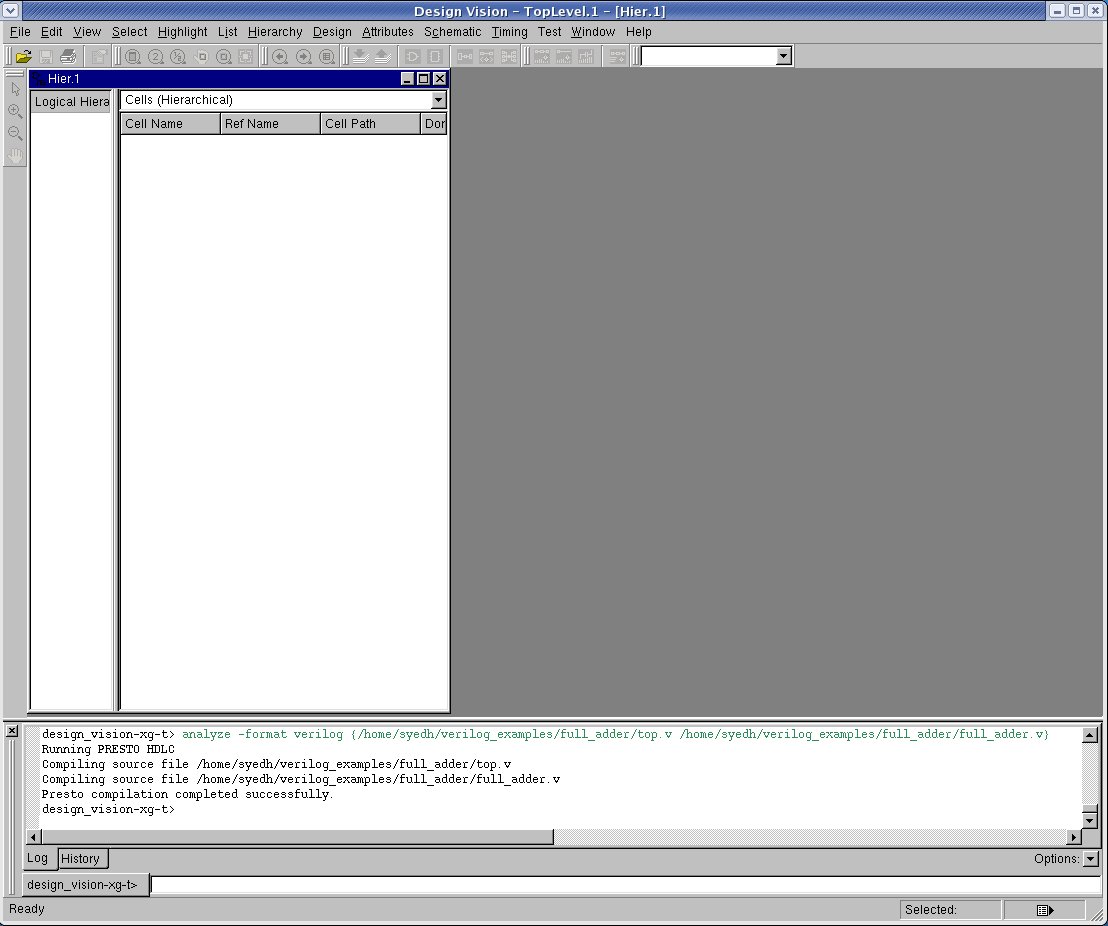
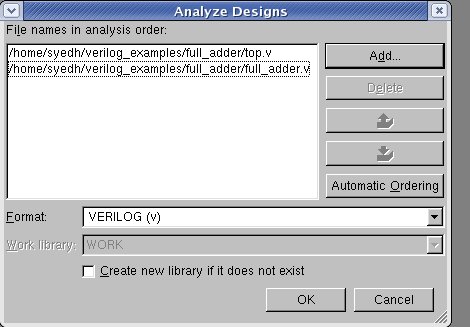
In Menu: File --> Analyze. A Dialog box will appear called “Analyze Designs”. Click the “Add..” button and add every design file {full_adder.v top.v}. You can do this one file at a time or all at one time by using the CTRL key to select multiple files. After adding all the files press OK.
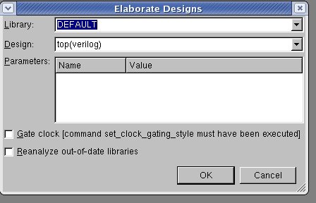
In Menu: Design --> Elaborate.
A Dialog box will appear called “Elaborate Designs”. There will be a drop down selection menu called “Design”. In this selection menu there will be two objects listed: top(verilog) and full_adder(verilog). Make sure that top(verilog) is selected. Press OK.
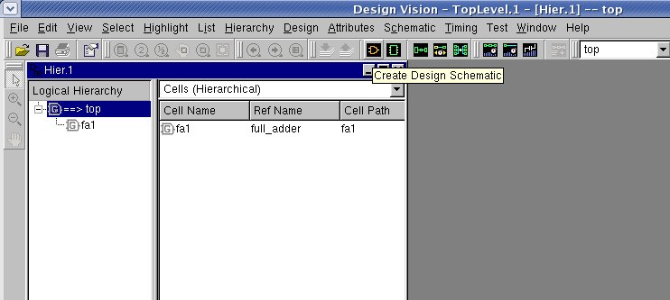
Now in the Design Vision the “Hier 1” window will have objects listed in it.
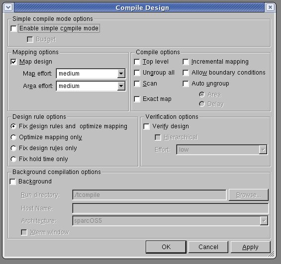
In Menu: Design --> Compile. In the dialog box that shows up press OK. After doing this your design will now have parts from the library in it.
In Menu: File --> Save As. Save the design as a verilog design with a new name (ex. top_syn.v).
9. Exit the gui and in the command prompt type exit to quit out of the design_vision_xg_t shell. Then type exit again to quit Synopsys.
Simulate Design and Get Switching Activity (VCD file)
10. Now it is time to simulate the synthesized design, top_syn.v, with the testbench, tb_top.v. The verilog simulator program of Synopsys is called VCX. The first step is to write a script for the simulation:
#vcs_script.scr
#This is a script file for VCX simulator
./tb_top.v
./top_syn.v
-v ./iit018_stdcells.v
+libext+.v +nolibcell +define+VPD+SAIF+VCD+SDF
11. At command prompt type:
Synopsys
Now type:
vcs -f vcs_script.scr
The result of running this command is that an executable called simv is created.
12. Run simv :
./simv
13. Now the file dmp_top.vcd has been created.
Power Estimation with Synopsys PrimeTime-PX
14. Now we will use a tool called PrimeTime-Px to get power estimation. The following script called power.scr will be used.
#power.scr
set power_enable_analysis TRUE
set target_library "/home/syedh/iit_stdcells/lib/tsmc018/lib/iit018_stdcells.db"
set link_library "/home/syedh/iit_stdcells/lib/tsmc018/lib/iit018_stdcells.db *"

read_db $target_library
read_verilog top_syn.v
current_design top
link
read_vcd dmp_top.vcd -strip_path tb_top/uut
create_power_waveforms –output vcd
report_power
15. At the Synopsys command prompt type:
pt_shell
Now run the power.scr:
source power.scr
16. If all went right the output from the script should look something like this:
======================================================================
Summary:
Total number of nets = 11
Number of annotated nets = 11 (100.00%)
Total number of leaf cells = 7
Number of fully annotated leaf cells = 7 (100.00%)
======================================================================

Information: The waveform options are:
                File name:      power_waves.fsdb
                File format:    fsdb
                Time interval:  0.01ns
                Hierarchical level:     all

Information: Power analysis is running, please wait ...

Information: analysis is done for time window (0ns - 5050ns)

****************************************
Report : Event Based Power
Design : top
Version: Z-2007.06-SP3
Date   : Wed Feb 13 14:34:11 2008
****************************************


  Attributes
  ----------
      i  -  Including register clock pin internal power
      u  -  User defined power group

                        Internal  Switching  Leakage    Total
Power Group             Power     Power      Power      Power   (     %)  Attrs
--------------------------------------------------------------------------------
io_pad                     0.0000    0.0000    0.0000    0.0000 ( 0.00%)
memory                     0.0000    0.0000    0.0000    0.0000 ( 0.00%)
black_box                  0.0000    0.0000    0.0000    0.0000 ( 0.00%)
clock_network           3.292e-06    0.0000    0.0000 3.292e-06 (58.67%)  i
register                6.722e-07 4.735e-07 4.822e-10 1.146e-06 (20.42%)
combinational           8.640e-07 3.086e-07 4.037e-10 1.173e-06 (20.90%)
sequential                 0.0000    0.0000    0.0000    0.0000 ( 0.00%)

 Net Switching Power  = 7.821e-07   (13.94%)
 Cell Internal Power  = 4.828e-06   (86.05%)
 Cell Leakage Power   = 8.859e-10   ( 0.02%)
                         ---------
Total Power            = 5.611e-06  (100.00%)

X Transition Power     =    0.0000
Glitching Power        = 2.152e-08

Peak Power             = 4.726e-03
Peak Time              =   550.100
